Recently, the University of Science and Technology of China team has made important progress in the field of gallium oxide power electronic devices.
The research group of Professor Long Shibing from the School of Microelectronics of the University of Science and Technology of China has successfully fabricated a gallium oxide heterojunction diode with high voltage resistance and high temperature resistance, and a gallium oxide enhanced heterojunction field effect transistor. Two related papers were selected into the 34th International Conference on Power Semiconductor Devices and Integrated Circuits ISPSD.
The rapid development of energy, information, national defense, rail transportation, electric vehicles and other fields has put forward higher requirements for the performance of power semiconductor devices, and high withstand voltage, low loss, and high power devices have become the future development trend. As a new-generation power semiconductor material, gallium oxide has a large band gap and strong resistance to extreme environments, and is expected to play an important role in the field of future power devices. The forbidden band width of semiconductors is an important characteristic parameter of semiconductors, and its size mainly depends on the energy band structure of the semiconductors, that is, it is related to the crystal structure and the bonding properties of atoms. However, there are still many problems in the industrialization of gallium oxide power semiconductor devices, including the difficulty of suppressing the edge peak electric field and the difficulty of realizing enhancement mode transistors.
The research group of Long Shibing of the University of Science and Technology of China has conducted researches on the aforementioned two pain points respectively.
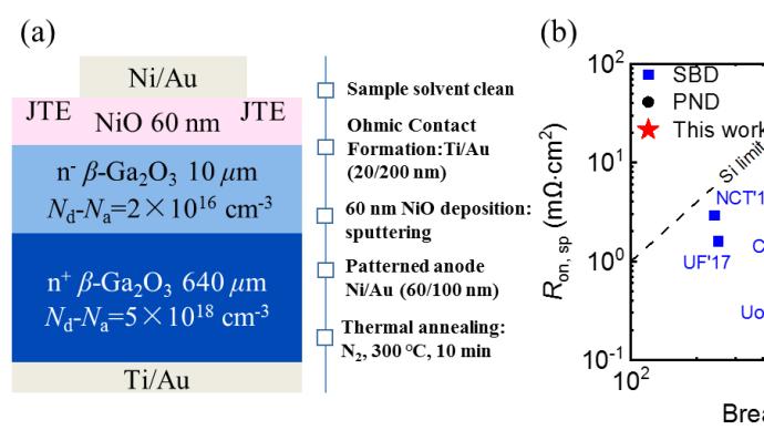
At present, due to the challenges of gallium oxide P-type doping, the gallium oxide homogenous PN junction as an extremely important basic device is temporarily difficult to achieve, resulting in the lack of gallium oxide diode devices that use a homogenous PN junction to suppress the peak electric field at the edge of the anode (such as field ring, junction terminal extension, etc.). To this end, the use of other suitable P-type oxide materials to form a heterojunction with gallium oxide is a feasible solution. P-type semiconductor NiO (nickel oxide) is a good choice due to its large band gap and controllable doping.
Based on the NiO growth process and the previous research foundation of hetero-PN, the aforementioned research group designed a junction termination extension structure (JTE) and optimized the annealing process to successfully fabricate a high-voltage and high-temperature-resistant gallium oxide heterojunction diode. The JTE design used in this study can effectively alleviate the fringe electric field aggregation effect of the NiO/Ga2O3 (gallium oxide) junction and improve the breakdown voltage of the device. The annealing process can greatly reduce the reverse leakage current of the heterojunction and improve the current switching ratio. The final test results show that the device has a low on-resistance of 2.5mΩ·cm^2 (mΩ is milliohms) and a high breakdown voltage of 2.66kV (kilovolt) at room temperature, and its power quality factor is as high as 2.83GW/cm^2 (GW is gigawatts). In addition, the device can still maintain a breakdown voltage of 1.77kV at 250 degrees Celsius, showing good high-temperature blocking characteristics, which is the first reported high-temperature breakdown characteristic in the field.
In response to the aforementioned problems, Long Shibing's research group introduced P-type NiO, which is also a wide-bandgap semiconductor material, based on the original enhancement-mode transistor design, and combined it with the trench-type structure to successfully design and prepare a gallium oxide-enhanced transistor. Heterojunction field effect transistors. The device achieves a threshold voltage of 0.9V (volts), low subthreshold swing, high device transconductance, and near-zero device hysteresis characteristics, which indicate good gate control capabilities. In addition, the on-resistance of the device is well maintained at 151.5Ω·mm (Ω is ohm, mm is millimeter), and the breakdown voltage reaches 980V.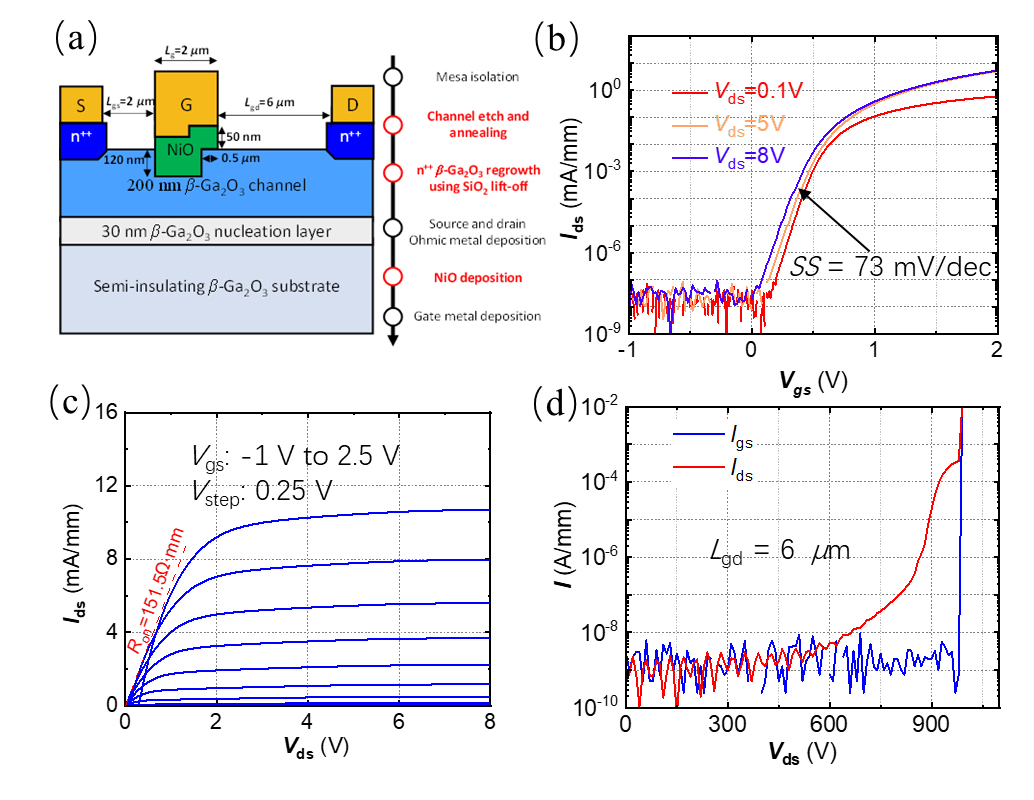
The research group of Professor Long Shibing from the School of Microelectronics of the University of Science and Technology of China has successfully fabricated a gallium oxide heterojunction diode with high voltage resistance and high temperature resistance, and a gallium oxide enhanced heterojunction field effect transistor. Two related papers were selected into the 34th International Conference on Power Semiconductor Devices and Integrated Circuits ISPSD.
The rapid development of energy, information, national defense, rail transportation, electric vehicles and other fields has put forward higher requirements for the performance of power semiconductor devices, and high withstand voltage, low loss, and high power devices have become the future development trend. As a new-generation power semiconductor material, gallium oxide has a large band gap and strong resistance to extreme environments, and is expected to play an important role in the field of future power devices. The forbidden band width of semiconductors is an important characteristic parameter of semiconductors, and its size mainly depends on the energy band structure of the semiconductors, that is, it is related to the crystal structure and the bonding properties of atoms. However, there are still many problems in the industrialization of gallium oxide power semiconductor devices, including the difficulty of suppressing the edge peak electric field and the difficulty of realizing enhancement mode transistors.
The research group of Long Shibing of the University of Science and Technology of China has conducted researches on the aforementioned two pain points respectively.
At present, due to the challenges of gallium oxide P-type doping, the gallium oxide homogenous PN junction as an extremely important basic device is temporarily difficult to achieve, resulting in the lack of gallium oxide diode devices that use a homogenous PN junction to suppress the peak electric field at the edge of the anode (such as field ring, junction terminal extension, etc.). To this end, the use of other suitable P-type oxide materials to form a heterojunction with gallium oxide is a feasible solution. P-type semiconductor NiO (nickel oxide) is a good choice due to its large band gap and controllable doping.
Based on the NiO growth process and the previous research foundation of hetero-PN, the aforementioned research group designed a junction termination extension structure (JTE) and optimized the annealing process to successfully fabricate a high-voltage and high-temperature-resistant gallium oxide heterojunction diode. The JTE design used in this study can effectively alleviate the fringe electric field aggregation effect of the NiO/Ga2O3 (gallium oxide) junction and improve the breakdown voltage of the device. The annealing process can greatly reduce the reverse leakage current of the heterojunction and improve the current switching ratio. The final test results show that the device has a low on-resistance of 2.5mΩ·cm^2 (mΩ is milliohms) and a high breakdown voltage of 2.66kV (kilovolt) at room temperature, and its power quality factor is as high as 2.83GW/cm^2 (GW is gigawatts). In addition, the device can still maintain a breakdown voltage of 1.77kV at 250 degrees Celsius, showing good high-temperature blocking characteristics, which is the first reported high-temperature breakdown characteristic in the field.
Figure 1. Junction termination extended NiO/β-Ga2O3 heterojunction diode (a) schematic cross-section and key fabrication details of the device, (b) performance comparison with reported gallium oxide Schottky diodes and heterojunction diodes, the picture comes from University of Science and Technology of China
In terms of enhancement mode transistors, they have a self-protection function of false turn-on and only need a single power supply, so enhancement mode devices are usually selected in power applications. However, due to the lack of gallium oxide P-type doping technology, field effect transistors are generally depletion-mode devices, and enhancement-mode structures are difficult to design and implement. Common enhancement designs tend to significantly increase the on-resistance of the device, resulting in excessive conduction losses.In response to the aforementioned problems, Long Shibing's research group introduced P-type NiO, which is also a wide-bandgap semiconductor material, based on the original enhancement-mode transistor design, and combined it with the trench-type structure to successfully design and prepare a gallium oxide-enhanced transistor. Heterojunction field effect transistors. The device achieves a threshold voltage of 0.9V (volts), low subthreshold swing, high device transconductance, and near-zero device hysteresis characteristics, which indicate good gate control capabilities. In addition, the on-resistance of the device is well maintained at 151.5Ω·mm (Ω is ohm, mm is millimeter), and the breakdown voltage reaches 980V.
Fig.2 Based on hetero-PN gallium oxide junction field effect transistor (a) structural schematic diagram and process flow diagram, (b) transfer characteristics of different drain biases, (c) output characteristic curves, and (d) breakdown characteristic curves , the picture comes from the University of Science and Technology of China
Related Posts
0 Comments
Write A Comments